A BJT is a current-driven semiconductor device. For switching work, the goal is usually a clean OFF state and a well-driven saturated ON state. Load connects to positive supply.
The main ideas are: Load connects to positive supply. Transistor collector connects to load. Emitter returns to ground. Base resistor controls the device. Inductive loads need a flyback path.
Do not design a BJT switch from a typical DC current gain number alone. Switching requires margin. Estimate load current, choose a reasonable forced beta, calculate base current, verify the control source can provide it, and then check saturation loss and device heating.
The safest design usually has an intentional answer to three questions: what happens at startup, what happens during a fault, and where stored energy goes at turn-off.
Worked thinking: A 12 V solenoid can be switched by an NPN transistor if collector current, base drive, power, and flyback protection are all adequate. The example is meant to demonstrate the method, not to replace the ratings and test conditions of the actual part you use.
Design view – load connects to positive supply. Ask which component or connection establishes this behavior and which rating could be exceeded if the load changes. This turns a descriptive fact into a selection rule.
Troubleshooting view – transistor collector connects to load. Imagine the reading if this condition were missing, too weak, too high, reversed, or intermittent. A useful test is one that separates those possibilities instead of merely producing another number.
Design view – emitter returns to ground. Ask which component or connection establishes this behavior and which rating could be exceeded if the load changes. This turns a descriptive fact into a selection rule.
Troubleshooting view – base resistor controls the device. Imagine the reading if this condition were missing, too weak, too high, reversed, or intermittent. A useful test is one that separates those possibilities instead of merely producing another number.
Design view – inductive loads need a flyback path. Ask which component or connection establishes this behavior and which rating could be exceeded if the load changes. This turns a descriptive fact into a selection rule.
A switch should be evaluated in both steady state and transition state. ON-state voltage drop creates heat, OFF-state voltage stress can damage the device, and the brief transition between states can be the most stressful period during fast or repetitive switching.
Finish by verifying the real load. A driver that works with an LED may still fail with a relay, motor, solenoid, heater, or long cable because startup current, inductance, wiring resistance, and electrical noise change the conditions dramatically.
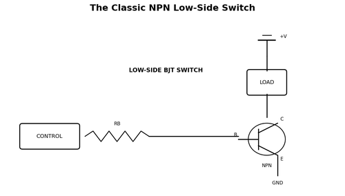
Worked Example
A 12 V solenoid can be switched by an NPN transistor if collector current, base drive, power, and flyback protection are all adequate.
Hands-On Mini-Lab
- Identify base collector and emitter from a reliable pinout.
- Use diode-test mode to inspect the base junctions.
- Calculate a base resistor for a safe low-current load.
- Measure base current and VCE while ON.
- Compare measured transistor heating with the calculated power loss.
Common Beginner Mistakes
- Choosing the base resistor from typical transistor gain.
- Forgetting the base resistor entirely.
- Ignoring VCE(sat) and transistor heating.
- Confusing NPN and PNP polarity.
Fault-Finding Lens
- Verify the actual supply voltage at the load and switching device while the load is commanded ON.
- Measure the control quantity at the device itself: base current for a BJT, VGS for a MOSFET, or coil voltage for a relay.
- Check the load independently when possible so a failed load is not mistaken for a failed driver.
- Inspect protection parts, grounds, connectors, and wiring for open circuits, shorts, reversed polarity, or excessive voltage drop.
- After the repair, repeat the original operating condition and verify current, voltage drop, temperature, and turn-off behavior.
Check Your Understanding
- Explain the classic npn low-side switch in your own words.
- Which voltage or current would you measure first to verify this stage?
- What is one failure mode that could make the switch run hot?
- What protection component or design margin is most relevant here?
- How would the circuit behave during controller startup or reset?
Key Points
- Load connects to positive supply.
- Transistor collector connects to load.
- Emitter returns to ground.
- Base resistor controls the device.
- Inductive loads need a flyback path.