A BJT is a current-driven semiconductor device. For switching work, the goal is usually a clean OFF state and a well-driven saturated ON state. Emitter voltage follows base voltage minus a junction drop.
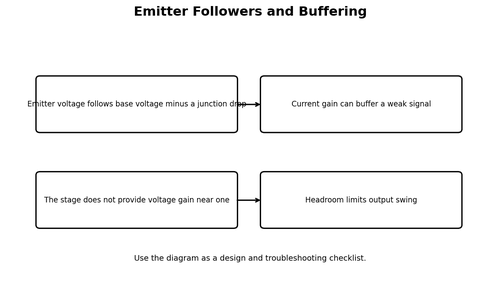
The main ideas are: Emitter voltage follows base voltage minus a junction drop. Current gain can buffer a weak signal. The stage does not provide voltage gain near one. Headroom limits output swing.
Do not design a BJT switch from a typical DC current gain number alone. Switching requires margin. Estimate load current, choose a reasonable forced beta, calculate base current, verify the control source can provide it, and then check saturation loss and device heating.
Think of the switch as a controlled door in the load-current path. The control signal decides when the door opens, but the door itself must survive the traffic passing through it.
Worked thinking: A 3 V base signal may produce roughly 2.3 V at the emitter under appropriate load conditions. The example is meant to demonstrate the method, not to replace the ratings and test conditions of the actual part you use.
Design view – emitter voltage follows base voltage minus a junction drop. Ask which component or connection establishes this behavior and which rating could be exceeded if the load changes. This turns a descriptive fact into a selection rule.
Troubleshooting view – current gain can buffer a weak signal. Imagine the reading if this condition were missing, too weak, too high, reversed, or intermittent. A useful test is one that separates those possibilities instead of merely producing another number.
Design view – the stage does not provide voltage gain near one. Ask which component or connection establishes this behavior and which rating could be exceeded if the load changes. This turns a descriptive fact into a selection rule.
Troubleshooting view – headroom limits output swing. Imagine the reading if this condition were missing, too weak, too high, reversed, or intermittent. A useful test is one that separates those possibilities instead of merely producing another number.
A switch should be evaluated in both steady state and transition state. ON-state voltage drop creates heat, OFF-state voltage stress can damage the device, and the brief transition between states can be the most stressful period during fast or repetitive switching.
Finish by verifying the real load. A driver that works with an LED may still fail with a relay, motor, solenoid, heater, or long cable because startup current, inductance, wiring resistance, and electrical noise change the conditions dramatically.
Worked Example
A 3 V base signal may produce roughly 2.3 V at the emitter under appropriate load conditions.
Hands-On Mini-Lab
- Identify base collector and emitter from a reliable pinout.
- Use diode-test mode to inspect the base junctions.
- Calculate a base resistor for a safe low-current load.
- Measure base current and VCE while ON.
- Compare measured transistor heating with the calculated power loss.
Common Beginner Mistakes
- Ignoring VCE(sat) and transistor heating.
- Confusing NPN and PNP polarity.
- Choosing the base resistor from typical transistor gain.
- Forgetting the base resistor entirely.
Fault-Finding Lens
- Verify the actual supply voltage at the load and switching device while the load is commanded ON.
- Measure the control quantity at the device itself: base current for a BJT, VGS for a MOSFET, or coil voltage for a relay.
- Check the load independently when possible so a failed load is not mistaken for a failed driver.
- Inspect protection parts, grounds, connectors, and wiring for open circuits, shorts, reversed polarity, or excessive voltage drop.
- After the repair, repeat the original operating condition and verify current, voltage drop, temperature, and turn-off behavior.
Check Your Understanding
- Explain emitter followers and buffering in your own words.
- Which voltage or current would you measure first to verify this stage?
- What is one failure mode that could make the switch run hot?
- What protection component or design margin is most relevant here?
- How would the circuit behave during controller startup or reset?
Key Points
- Emitter voltage follows base voltage minus a junction drop.
- Current gain can buffer a weak signal.
- The stage does not provide voltage gain near one.
- Headroom limits output swing.