A MOSFET is controlled mainly by gate-to-source voltage, but real designs must also account for gate charge, resistance, transient voltage, and heat. The gate is insulated and draws little steady dc current.
The main ideas are: The gate is insulated and draws little steady dc current. Drain-source current is controlled by gate-to-source voltage. The intrinsic body diode creates a directional path. N-channel and p-channel devices use opposite polarities.
Do not ask only whether the gate voltage exceeds threshold. Ask what RDS(on) is specified at the actual VGS you will provide, how much current flows, what transient voltage exists, how quickly the gate is charged, and whether the thermal path can remove the resulting heat.
Think of the switch as a controlled door in the load-current path. The control signal decides when the door opens, but the door itself must survive the traffic passing through it.
Worked thinking: A power N-channel MOSFET can remain off with drain at 12 V and source at ground until its gate is driven positive relative to source. The example is meant to demonstrate the method, not to replace the ratings and test conditions of the actual part you use.
Design view – the gate is insulated and draws little steady DC current. Ask which component or connection establishes this behavior and which rating could be exceeded if the load changes. This turns a descriptive fact into a selection rule.
Troubleshooting view – drain-source current is controlled by gate-to-source voltage. Imagine the reading if this condition were missing, too weak, too high, reversed, or intermittent. A useful test is one that separates those possibilities instead of merely producing another number.
Design view – the intrinsic body diode creates a directional path. Ask which component or connection establishes this behavior and which rating could be exceeded if the load changes. This turns a descriptive fact into a selection rule.
Troubleshooting view – N-channel and P-channel devices use opposite polarities. Imagine the reading if this condition were missing, too weak, too high, reversed, or intermittent. A useful test is one that separates those possibilities instead of merely producing another number.
A switch should be evaluated in both steady state and transition state. ON-state voltage drop creates heat, OFF-state voltage stress can damage the device, and the brief transition between states can be the most stressful period during fast or repetitive switching.
Finish by verifying the real load. A driver that works with an LED may still fail with a relay, motor, solenoid, heater, or long cable because startup current, inductance, wiring resistance, and electrical noise change the conditions dramatically.
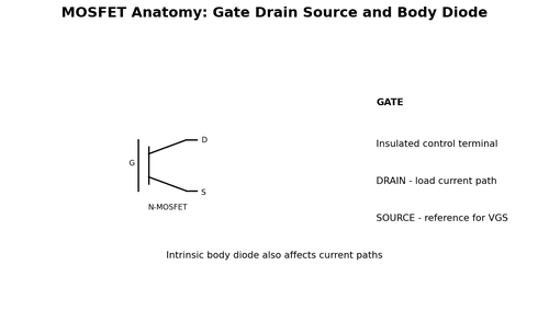
Worked Example
A power N-channel MOSFET can remain off with drain at 12 V and source at ground until its gate is driven positive relative to source.
Hands-On Mini-Lab
- Identify gate drain and source from the datasheet.
- Verify the gate has a pull resistor that defines OFF.
- Measure VGS rather than gate-to-ground voltage alone.
- Measure load current and voltage drop across the MOSFET.
- Estimate conduction loss and observe temperature after several minutes.
Common Beginner Mistakes
- Ignoring switching loss during PWM.
- Using VGS(th) as the fully-on voltage.
- Leaving the gate floating.
- Choosing only by headline drain-current rating.
Fault-Finding Lens
- Verify the actual supply voltage at the load and switching device while the load is commanded ON.
- Measure the control quantity at the device itself: base current for a BJT, VGS for a MOSFET, or coil voltage for a relay.
- Check the load independently when possible so a failed load is not mistaken for a failed driver.
- Inspect protection parts, grounds, connectors, and wiring for open circuits, shorts, reversed polarity, or excessive voltage drop.
- After the repair, repeat the original operating condition and verify current, voltage drop, temperature, and turn-off behavior.
Check Your Understanding
- Explain mosfet anatomy: gate drain source and body diode in your own words.
- Which voltage or current would you measure first to verify this stage?
- What is one failure mode that could make the switch run hot?
- What protection component or design margin is most relevant here?
- How would the circuit behave during controller startup or reset?
Key Points
- The gate is insulated and draws little steady dc current.
- Drain-source current is controlled by gate-to-source voltage.
- The intrinsic body diode creates a directional path.
- N-channel and p-channel devices use opposite polarities.